Author: raoam488

  • AI Designs Microstructured Materials for Optimized Optics and Heat Control

    AI Designs Microstructured Materials for Optimized Optics and Heat Control

    Researchers have developed a novel artificial intelligence framework to significantly accelerate the design of advanced materials with specific optical properties. This innovative system combines several neural networks to rapidly predict and optimize the characteristics of microstructured materials, overcoming the limitations of traditional simulation methods which can be computationally intensive and time-consuming.

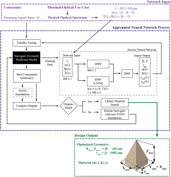
    The new framework utilizes a four-stage process. It begins with data generated from Finite-Difference Time-Domain (FDTD) simulations, a method for precisely modeling light-matter interactions. This data is then used to train a “surrogate” neural network, which acts as a fast predictor of optical properties for various materials. This surrogate network rapidly assesses a wide range of materials, generating predictions that then train a second “inverse” neural network.

    The inverse network is the core of the design tool. It takes a desired optical spectrum – essentially the blueprint of how light should interact with the material in terms of wavelength, emissivity, reflectivity, and transmissivity – as input. It then predicts the optimal physical structure of the material, including the dimensions of micropyramids on its surface and the material composition (specifically, the complex refractive index).

    A crucial “post-processing” module is incorporated to ensure the practicality of the design. This module interprets the output of the inverse network and applies real-world constraints, such as limitations on the aspect ratio of the microstructure (how tall it is compared to its width) to ensure the designs are manufacturable. If the initial solution doesn’t meet these constraints, the system automatically adjusts the design to find viable alternatives. The adjusted solutions are then re-evaluated using both FDTD and the surrogate model to ensure accuracy. The system is designed to iteratively refine its predictions; if discrepancies are found between the desired optical properties and the achieved ones, or between the surrogate model’s prediction and the more accurate FDTD simulations, the surrogate network can be retrained with new data to improve its future performance.

    The researchers emphasize the effectiveness of the surrogate neural network. They have developed two versions: a deep neural network (DNN) and a convolutional deep neural network (CDNN). Both are trained on data from FDTD simulations of micropyramid structures. The DNN directly processes geometric and material inputs to predict optical properties, demonstrating rapid prediction speeds and good accuracy, even when dealing with materials not explicitly included in its training data. The CDNN takes a different approach, analyzing a visual representation of the material structure, mimicking how an FDTD solver works by considering material properties across a discretized mesh. This image-based method proves to be even more accurate in predicting properties for new materials, especially when limited training data is available.

    The inverse neural network, built upon the speed of the surrogate network, is designed to solve the “inverse problem” – determining the material and structure needed to achieve a specific optical response. It analyzes the full spectral distribution of desired optical properties and outputs the corresponding geometric parameters and material properties. Tests using target spectra for ideal heating, cooling, and unity emissivity demonstrate the network’s capability to generate functional designs, even for complex and potentially physically challenging target optical responses.

    While the inverse network excels at design, it doesn’t inherently incorporate manufacturing constraints. The post-processing module addresses this by allowing users to set limitations, such as maximum aspect ratios, which are crucial for real-world fabrication. This module refines the initial network output, searching for alternative, manufacturable designs that still closely match the desired optical performance. This iterative process involves adjusting the geometry, re-simulating with the surrogate model, and verifying the best solutions with FDTD, ensuring the final designs are both practical and effective.

    The aggregated neural network system is designed to be self-improving. By continuously comparing its predictions with accurate simulations and real-world constraints, and incorporating new data, the system learns and refines its design capabilities over time. This technology holds significant promise for accelerating innovation in various fields, including energy management, thermal control, and advanced optical devices, by enabling rapid and efficient design of metamaterials tailored to specific needs.

    Source link

  • Simple Layered Designs Boost Efficiency of Optical Concentrators

    Simple Layered Designs Boost Efficiency of Optical Concentrators

    Scientists have engineered a novel approach to focus electromagnetic fields using specially designed materials arranged in layers. This breakthrough, rooted in the theoretical understanding of how light behaves, paves the way for advancements in optical technology.

    Researchers detailed a method for creating a ‘field concentrator’ by carefully structuring layers of two semiconductor materials, AlInAs and InGaAs. This layered design, functioning as a metamaterial, manipulates electromagnetic waves in a unique way. The core idea involves compressing and extending the space through which light travels, effectively squeezing the electromagnetic field into a smaller region, thereby increasing its intensity.

    Through rigorous simulations, the scientists demonstrated that their layered concentrator effectively enhances the electromagnetic field within its core. The design also showed a reduction in unwanted scattering of light, making it nearly invisible to incoming waves. Importantly, this approach is functional across a range of wavelengths, offering versatility for different applications.

    Even when accounting for material losses that occur in real-world materials, the concentrator maintained its ability to focus fields, proving its potential for practical applications. This new method, utilizing readily available semiconductor materials and a layered architecture, presents a significant step forward in creating efficient and functional electromagnetic field concentrators for advanced optical devices.

    Source link

  • Ford Optical Illusion Thwarts ‘Selfie Spies’ Stealing Car Designs

    Ford is using optical illusions to protect its new car designs from prying eyes, particularly those of “selfie spies.” The automaker has implemented a unique camouflage at its design studios that distorts the shapes and lines of vehicles under development, making it difficult for unauthorized individuals to photograph and leak sensitive design details. This innovative approach reportedly uses deceptive patterns and visual tricks to confuse cameras and the human eye, ensuring that future Ford models remain secret until their official unveiling. The system aims to safeguard Ford’s intellectual property and maintain a competitive edge in the automotive market by preventing early leaks of design aesthetics.

    Source link

  • Tape Op Magazine Reviews Grace Design m502 Optical Compressor

    Grace Design has released the m502, a new 500-series optical compressor module. Known for their high-fidelity audio equipment, Grace Design built the m502 as a 500-series version of a “full-rack” compressor, emphasizing pristine sound and professional features. The m502 includes standard controls such as threshold, attack, release, compression ratio, and output level, alongside a compression activation switch and peak LED. Standout features include a stepped input stage, stereo-link capability, selectable external sidechain activation, compatibility with Radial Engineering Workhorse and Purple Audio Sweet Ten chassis, and a large 10-segment LED gain-reduction meter. Despite a minimalist front panel design, the m502 is reported to be user-friendly, especially with its responsive gain-reduction meter. Sound quality is described as natural, vibey, and smooth, maintaining clarity even at higher compression settings. The compressor is praised for its versatility and effectiveness in various applications, from vocals and bass to drums and acoustic instruments, as well as on the mix bus. Users highlight its ability to transparently manage dynamics and add punch without sacrificing detail. Stereo linking functionality is also noted as effective for stereo sources. Overall, the m502 is presented as a high-fidelity and versatile compressor suited for professional studio use, considered a valuable addition to any 500-series rack. The Grace Design m502 optical compressor is priced at $625 street and available through www.gracedesign.com.

    Source link

  • Option 1 (Focus on AI/Inverse Design):

AI Designs Ultra-Compact Diode for Broadband One-Way Light Flow

Option 2 (Focus on Compactness & Function):

Ultra-Compact Optical Diode Achieves Broadband, One-Way Light Control

Option 3 (Slightly more technical, but still concise):

Inverse Design Yields Tiny Broadband Optical Diode for Directional Light

Option 4 (Emphasis on Breakthrough):

Breakthrough: Ultra-Compact Broadband Optical Diode Controls Light Direction

Option 5 (Shortest, most impactful):

Tiny Optical Diode Enables Broadband One-Way Light Flow

All options are under 13 words and suitable for news headlines. Option 1 and 2 are probably the strongest in terms of being informative and engaging as news. Let’s go with Option 1:

AI Designs Ultra-Compact Diode for Broadband One-Way Light Flow

    Option 1 (Focus on AI/Inverse Design):

    AI Designs Ultra-Compact Diode for Broadband One-Way Light Flow

    Option 2 (Focus on Compactness & Function):

    Ultra-Compact Optical Diode Achieves Broadband, One-Way Light Control

    Option 3 (Slightly more technical, but still concise):

    Inverse Design Yields Tiny Broadband Optical Diode for Directional Light

    Option 4 (Emphasis on Breakthrough):

    Breakthrough: Ultra-Compact Broadband Optical Diode Controls Light Direction

    Option 5 (Shortest, most impactful):

    Tiny Optical Diode Enables Broadband One-Way Light Flow

    All options are under 13 words and suitable for news headlines. Option 1 and 2 are probably the strongest in terms of being informative and engaging as news. Let’s go with Option 1:

    AI Designs Ultra-Compact Diode for Broadband One-Way Light Flow

    Researchers have developed a novel optimization algorithm to streamline the design of photonic devices, which are crucial components in technologies that manipulate light, such as advanced communication systems and sensors. Designing these devices traditionally involves a complex and time-consuming trial-and-error process. Engineers would manually propose a structure, simulate its interaction with light, and then tweak the design based on the simulation results. This process is not only inefficient but also relies heavily on intuition and limited automated methods.

    The new algorithm approaches the design problem by treating the device as a “black box” and directly optimizing for a desired light output. Instead of iteratively guessing structures, the algorithm works backward from the intended device function, such as specific spectral modulation or mode conversion. It mathematically defines the device’s objective, for example, achieving a particular magnetic field at its boundaries. Then, it iteratively refines both the device’s internal dielectric structure and the electromagnetic fields within it to match this objective, while simultaneously adhering to the fundamental laws of electromagnetism, known as Maxwell’s equations.

    This iterative process is broken down into two steps. First, it assumes a dielectric structure and calculates the electromagnetic field that minimizes discrepancies within Maxwell’s equations. Second, it reverses the roles, optimizing the dielectric structure based on the previously calculated electromagnetic field. These steps are repeated, gradually converging toward a design that fulfills the objective. This “objective-first” approach is significantly faster and less computationally demanding than traditional methods, and it can handle more complex designs with greater freedom.

    A key challenge in practical photonics is that devices are typically made from a limited number of materials, often just two, like silicon and air, creating a binary structure. The initial optimization algorithm generates structures with continuous variations in material properties, which are not directly fabricable. To address this, the researchers incorporated a “binarization” technique. This method encourages the algorithm to converge towards designs that are already close to a binary structure during the optimization process itself. By adding a cost function that favors binary solutions, the algorithm ensures that the device performance is maintained even when converted to a purely binary, manufacturable structure.

    To test and evaluate their algorithm, the researchers performed computer simulations in two dimensions, focusing on the behavior of Transverse Electric fields. They simulated device performance under various conditions and assessed it using metrics like the physics residual (a measure of how well the design adheres to Maxwell’s equations), transmission efficiency in both directions (left-to-right and right-to-left), and a “binary coefficient” indicating how close the designed structure is to a perfect binary structure. This new algorithm represents a significant step forward in automated photonic device design, promising faster development and potentially enabling more complex and efficient optical technologies.

    Source link

  • AI Designs Cheaper Optical Sensors, Boosting Research Affordability

    AI Designs Cheaper Optical Sensors, Boosting Research Affordability

    Researchers at UCLA have developed a low-cost, portable device that can detect proteins, cancer biomarkers, viruses, and other small objects. This innovation addresses the long-standing challenge of finding practical and affordable solutions for early diagnosis and treatment of serious diseases. The device utilizes plasmonic sensing, a technique that amplifies electric fields using metal nanostructures to detect molecules. Traditionally, plasmonic sensing has been limited to laboratory settings due to the requirement of expensive and bulky equipment. To overcome this limitation, the UCLA team employed machine learning to design a more efficient and cost-effective device.

    The prototype is lightweight and portable, featuring a 3D-printed housing, colored LEDs, and a camera. A machine learning algorithm was used to select the optimal combination of LEDs and develop a computational method for analyzing sensor output. This approach allows for a much more accurate and affordable sensor compared to conventional designs, making it accessible for wider use outside of research labs.

    The research team also developed flexible and disposable plasmonic sensors using new nanofabrication methods. These sensors can be modified to specifically target and capture molecules of interest like bacteria, viruses, or cancer cells by using a surface modification technique similar to a lock and key mechanism. To operate the device, a fluid sample such as blood or urine is applied to a disposable microchip containing the sensor. This chip is then inserted into the device, which automatically measures and provides the diagnostic results. The researchers suggest that this technology could be further miniaturized into a mobile phone attachment, leveraging smartphone capabilities for cloud connectivity and processing power, further reducing costs and increasing accessibility. This innovation aims to provide researchers and engineers with a tool to create optimized, low-cost optical sensors for various applications in healthcare and environmental monitoring.

    Source link

  • Meta Engineers Design High-Speed 100G Optical Connections

    Meta Engineers Design High-Speed 100G Optical Connections

    In a move to enhance data center performance and future-proof infrastructure, Facebook has announced the deployment of its newly developed 100 Gigabit per second (100G) single-mode optical transceiver solution across its data centers. This upgrade addresses the increasing demand for higher data rates while prioritizing power efficiency and cost-effectiveness.

    Previously relying on multi-mode fiber connections for 10 and 40 Gb/s speeds, Facebook encountered limitations in distance and future scalability. Upgrading to 100G using standard multi-mode transceivers would have required costly and time-consuming re-cabling with OM4 fiber, hindering long-term upgrades and flexibility. To overcome this, the company strategically shifted to single-mode fiber, traditionally used in telecommunications for long distances and high bandwidth, but often associated with higher power consumption and cost.

    Facebook engineered a solution tailored to data center environments, optimizing single-mode transceiver technology to meet specific needs. A comprehensive analysis revealed that the long-term savings from reduced fiber and patch panel usage with single-mode fiber outweighed the initial higher cost of transceivers. Further cost reductions were achieved by refining the transceiver specifications to match the specific demands of data centers.

    The resultant 100G single-mode optical transceiver solution prioritizes efficiency by adjusting specifications related to reach, temperature range, and service life, without compromising reliability. By adopting the CWDM4 MSA (Multi-Source Agreement) standard and modifying it for data center requirements, creating CWDM4-OCP, Facebook was able to leverage industry standards while optimizing for its specific application.

    Key modifications in the CWDM4-OCP specification include reducing the required reach from 2 kilometers to 500 meters and narrowing the operating temperature range from 0-70 degrees Celsius to 15-55 degrees Celsius, reflecting the controlled environment within data centers. These adjustments allow for significant efficiency gains and cost reductions while maintaining interoperability with standard CWDM4 specifications for shorter distances.

    This optimized 100G solution is already being deployed in Facebook’s data centers, with commercially available CWDM4-OCP modules identifiable by their distinctive “OCP green” pull tab. Navigating the challenges of being an early adopter of this technology, Facebook implemented rigorous testing and collaborated with a diverse supplier ecosystem, including both established and emerging manufacturers, to ensure successful large-scale deployment. By sharing the detailed specification, CWDM4-OCP, through the Open Compute Project (OCP), Facebook aims to foster wider adoption of this efficient and cost-effective 100G solution within the data center industry.

    Source link

  • Optical Components Now Integrated Into Existing Chip Designs

    Optical Components Now Integrated Into Existing Chip Designs

    Researchers have achieved a new milestone in chip technology by developing a method to integrate optical and electronic components on a single chip using standard manufacturing processes, but now with the capability to build them separately and optimize each independently. This breakthrough, led by teams from MIT, the University of California at Berkeley, and Boston University, overcomes limitations of their previous approach which required using older chip technology. The new technique allows the use of more modern, high-performance transistor technologies while incorporating photonics. By separating the fabrication of electronics and photonics, chip manufacturers could add optical input and output to processors and GPUs without significant changes to existing production lines, potentially boosting performance through faster speeds and reduced power consumption. Optical communication on chips is seen as essential for future computing needs as energy demands rise with increasing transistor counts. This integrated approach dramatically reduces the power consumption and space of optical components compared to current market options. The researchers utilized polysilicon, deposited directly on glass, and experimented with different deposition methods at SUNY Polytechnic Institute to find a balance between electrical conductivity and optical efficiency in the material. This advancement promises to pave the way for more energy-efficient and faster computer chips by merging the advantages of optical communication with advanced microelectronics.

    Source link

  • Optimized Design Method Boosts Free Space Optics Communication Systems

    Researchers have engineered a cutting-edge communication system that employs free space optics (FSO) technology. This innovative system transmits data wirelessly through the air, utilizing light similar to fiber optic cables but without the physical infrastructure. The design of this FSO system was achieved through a process of iterative optimization, a method that refines the system’s parameters repeatedly to enhance its performance and efficiency. This research suggests advancements in wireless communication capabilities, potentially leading to faster data transmission speeds and improved connectivity, particularly in scenarios where deploying traditional cable networks is challenging or costly. The developed system aims to optimize the design of wireless optical communication links for enhanced and reliable data transfer.

    Source link

  • Here are a few options for news article titles, keeping it under 13 words and news-style:

Lensless, Real-Time Beam Shaping Achieved: Optical Breakthrough (8 words)
Real-Time Beam Shaping Without Extra Optics: New Method Unveiled (10 words)
‘Lensless’ Beam Shaping Revolution: Instant Light Control Now Possible (10 words)
Breakthrough: Real-Time Beam Shaping Eliminates Need for Extra Optics (11 words)

I recommend "Lensless, Real-Time Beam Shaping Achieved: Optical Breakthrough". It’s concise, emphasizes the key innovation ("lensless" and "real-time"), and has a strong news headline feel by calling it a "breakthrough".

    Here are a few options for news article titles, keeping it under 13 words and news-style:

    1. Lensless, Real-Time Beam Shaping Achieved: Optical Breakthrough (8 words)
    2. Real-Time Beam Shaping Without Extra Optics: New Method Unveiled (10 words)
    3. ‘Lensless’ Beam Shaping Revolution: Instant Light Control Now Possible (10 words)
    4. Breakthrough: Real-Time Beam Shaping Eliminates Need for Extra Optics (11 words)

    I recommend "Lensless, Real-Time Beam Shaping Achieved: Optical Breakthrough". It’s concise, emphasizes the key innovation ("lensless" and "real-time"), and has a strong news headline feel by calling it a "breakthrough".

    Scientists have engineered a novel type of light-emitting diode display, known as OLED, capable of dynamically altering the shape of its light beam. This innovative technology stacks two OLED units vertically, allowing for independent control and emission. Unlike typical OLEDs with a uniform light projection, this new device can switch between a focused spot of light and a ring-shaped beam, or even create customized emission patterns.

    The device achieves this beam shaping by employing a unique driving system and a specially designed optical structure. By using alternating current and pulse width modulation, the two OLED units can be controlled with just two electrodes, simplifying the device architecture. The key to the beam shaping lies in the precise engineering of the internal layers of the OLED, creating what’s known as a microcavity. This microcavity is tailored to direct light emission in specific directions. One unit is designed for forward emission, projecting light straight ahead, while the other is optimized for sideward emission, creating the ring shape.

    Researchers demonstrated that by combining the emissions from both units, they can create a variety of beam shapes. Measurements confirmed a clear separation between the forward and sideward emission patterns, with the sideward emitting unit showing maximum intensity at an angle of 56 degrees. The technology boasts a rapid switching speed, capable of changing beam shapes in microseconds, making it suitable for high-speed applications.

    To ensure consistent color output across different beam shapes, the researchers employed different light-emitting materials for each OLED unit, compensating for inherent spectral shifts caused by the optical design. The versatility of the design was further validated by simulations showing its compatibility with various light-emitting materials, including quantum dots and perovskites, suggesting broad applicability across different display types.

    Furthermore, the team explored the use of simple external optical elements like lenses and prisms to further refine the beam shaping capabilities. Adding a half-sphere lens enhanced the contrast and focus of the light beam, while a prism allowed for the creation of asymmetric light patterns, demonstrating the potential for tailoring the light output for specific applications.

    This advancement in OLED technology opens up possibilities for advanced display systems with adaptable light projection, which could be beneficial in various fields requiring controlled illumination, such as specialized lighting, advanced imaging, and next-generation display technologies.

    Source link