Author: raoam488

  • Fiber Optics Design Precisely Measures NIF Beamline Performance

    Fiber Optics Design Precisely Measures NIF Beamline Performance

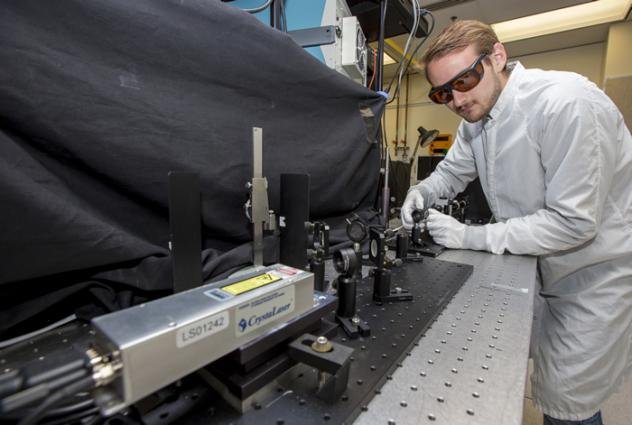
    Dylan Beckman, a 20-year-old optical engineering student from the University of Rochester, is contributing to the National Ignition Facility (NIF) this summer as a summer scholar. Beckman is designing new methods for transporting ultraviolet light via optical fiber cables from the Target Chamber to external diagnostic instruments at NIF. His designs have the potential to be implemented across all 192 of NIF’s laser beams.

    Beckman’s fascination with lasers began during a tour of the University of Rochester’s optical engineering building, leading him to switch his major from chemical engineering to optical engineering. His current work at NIF involves creating a more complex optical lens system to ease the load on optical fibers used to measure laser power. Mentors Abe Handler and Leyden Chang from the NIF Laser Diagnostics Group, along with Mike Messerly, Fiber Laser Group leader, have praised Beckman’s contributions. Messerly noted that Beckman’s designs are expected to simplify operations and improve efficiency at NIF.

    Currently, NIF measures power in only a quarter of its beamlines, relying on computer modeling for the remaining beams. Beckman is tasked with developing a system that could be deployed across all 192 beamlines, enhancing measurement accuracy and increasing confidence in laser performance for scientists and engineers. Handler explained that this upgrade is crucial for the future of NIF, as improved beamline information enables better system characterization and higher energy output.

    Beckman is developing physical prototypes of his system, aiming for a cost-effective design. Handler emphasized the significance of this project for the entire NIF facility and its users. While fiber optic cables are common in telecommunications, NIF requires specialized fibers capable of transmitting ultraviolet light and withstanding high-radiation environments. Messerly highlighted the challenges of using off-the-shelf solutions for NIF’s unique needs but noted that Beckman’s designs simplify the requirements for these custom fibers, potentially facilitating wider implementation across the facility.

    Handler acknowledged the complexity of NIF, especially for newcomers, but commended Beckman for his rapid skill acquisition and proactive approach. Beckman expressed his awe at the scale and complexity of NIF, describing it as a “giant well-oiled machine.” He is enthusiastic about contributing to such a large-scale project and hopes his system will be integrated into NIF, leaving a lasting impact on the world’s largest laser facility.

    Source link

  • Transparent Metal Films Power Next Generation See-Through Devices

    Researchers are exploring the advancements in transparent conductive materials, crucial components in various modern technologies such as touch screens, solar cells, and LED lighting. A significant area of focus involves thin metal films as a base for these transparent conductors. Recent studies delve into the methods of preparing these thin metal films, specifically examining different materials and techniques to achieve high transparency and conductivity. The optical design of these films is also a key consideration to maximize light transmission and minimize reflection, which are critical for device performance. Furthermore, the research highlights the diverse applications of these thin-metal-film-based transparent conductors across various electronic and optoelectronic devices, suggesting ongoing development and optimization efforts in this field to meet the growing demands of advanced technologies.

    Source link

  • Electro-Optical Circuit Board Advances Reported by I-Connect007

    Electro-Optical Circuit Board Advances Reported by I-Connect007

    January 22, 2025 – The future of circuit board design is poised for a significant shift away from traditional copper-based printed circuit boards (PCBs) as technology demands increasingly higher speeds and bandwidth. Limitations in copper PCBs, particularly in signal integrity at higher frequencies, are becoming more apparent, paving the way for innovative solutions like optical interconnects and photonic integrated circuits.

    Industry trends are driving demand for PCBs that are smaller, lighter, more flexible, and deliver significantly higher performance. This push has accelerated with the rise of artificial intelligence and the extreme data processing demands of leading-edge chips like NVIDIA’s Blackwell B200 GPU, which can operate at 720 petaflops and is interconnected with 800 Gbps networking.

    A major bottleneck in current high-speed systems lies within the copper interconnects themselves. Copper’s inherent limitations in speed and bandwidth are restricting the flow of data between ultra-fast devices. Since signal transmission in PCBs occurs within the dielectric material, not the copper traces, improving the efficiency of these dielectrics is crucial. However, even advanced low-loss dielectrics offer limited improvement, highlighting the fundamental constraints of copper.

    Electro-optical PCBs (EOCBs) emerge as a promising alternative, using light instead of electricity for data transmission. This approach offers superior signal integrity, faster speeds, and greater bandwidth capabilities. Optical interfaces also demonstrate greater energy efficiency at high data rates compared to their electrical counterparts. Furthermore, optical pathways provide enhanced isolation between board layers, ensuring uninterrupted signal transmission and boosting overall performance.

    EOCBs strategically integrate both optical and copper pathways; copper handles power distribution and lower-speed data, while optical paths manage high-speed signals. This hybrid approach addresses signal integrity issues common at high frequencies in copper systems, such as skin effect, crosstalk, and skew. Optical systems inherently avoid these problems, offering greater channel density and eliminating the need for signal conditioning and equalization, thus reducing power consumption. This integration also leads to a smaller PCB footprint, potentially reducing surface area by 20% and layer count by up to 50%.

    Flexible optical PCBs are also gaining traction, utilizing transparent materials like acrylic or clear epoxy and advanced photolithography and etching techniques to embed optical fibers or waveguides. These waveguides are crucial for modulating and transmitting light signals across the circuit pathways.

    High-speed optical interconnects leverage lasers, fiber optics, waveguides, and polarization components to create direct data pathways, minimizing delays and conversions. This ensures high bandwidth and reliable signal transmission. The goal is to achieve three-dimensional optical routing within PCBs using EOCBs and electro-optical transceivers.

    Photonic integrated circuits (PICs) are central to this evolution, acting as microchips containing multiple photonic components that generate, transport, detect, and process light. PIC technology drives the development of next-generation, miniaturized, high-performance devices through advanced features like distributed Bragg reflectors, dielectric waveguides, vertical couplers, and electro-optic modulators. This allows for unprecedented integration densities across applications from communications to sensing.

    Onboard optical interconnects can handle significantly higher data rates and channel counts compared to electrical interconnections while also being impervious to electromagnetic interference (EMI). This EMI immunity makes them particularly suitable for mixed-signal systems like data acquisition and sensitive sensor applications.

    Manufacturing optical PCBs requires careful consideration of waveguide fabrication, ensuring low signal attenuation and a reliable process compatible with existing PCB industry standards. This compatibility extends to assembly processes, needing coupling elements for optical signal input and output that can be automatically mounted using standard pick-and-place machines, ideally without requiring active alignment. Structured polymer foils are being explored to facilitate this integration.

    EOCB construction involves laminating low-cost glass sheets with conventional materials like FR-4. Glass can be used as a core layer or as a photonic interposer carrying PICs and electronic components. Copper plating is applicable to both glass and organic materials, maintaining compatibility with standard PCB processing, though high-precision assembly is necessary.

    Currently, challenges remain in connecting transceivers to the glass layer within EOCBs, specifically in routing photonic signals. Two main techniques are under development: using a periscope from the top or a small mirror from the bottom of the EOCB. However, industry-wide standards are yet to be established for these techniques.

    Developing EOCBs requires addressing design challenges across electrical (RF and electrical signal path optimization), optical (signal optimization, collimation, optomechanical system design), and thermal (heat source management and sink integration) domains.

    Fabricating waveguides within the glass layer of EOCBs is a critical technology, analogous to printing circuits on standard PCBs. Waveguides can be designed for single-mode (SM) or multi-mode (MM) transmission, with single-mode being favored in silicon photonics and multi-mode in datacom. Waveguides in glass can be created using lasers or ion exchange processes, with ion exchange offering the advantage of parallel processing.

    Looking ahead, EOCBs are expected to be crucial for future data processing needs, driven by the growing demands of AI and increasing data usage. Integrated optical connections will be vital at all levels, from chips to full panels. Waveguides made using ion-exchange processes in affordable display glass, laminated with conventional PCB materials, present a promising pathway to meet these needs and integrate optical conductors alongside traditional electrical routing.

    Source link
  • Here are a few options for rewriting the title as a news article headline, keeping it under 13 words:

Adaptive Algorithm Speeds Up Optical Metasurface Design (8 words)
New Algorithm Revolutionizes Optical Metasurface Design (7 words)
Adaptive Genetic Algorithm Boosts Optical Metasurface Design (9 words)
Smarter Algorithm for Faster Optical Metasurface Design Revealed (10 words)
Breakthrough: Adaptive Algorithm Streamlines Metasurface Design (8 words)

    Here are a few options for rewriting the title as a news article headline, keeping it under 13 words:

    1. Adaptive Algorithm Speeds Up Optical Metasurface Design (8 words)
    2. New Algorithm Revolutionizes Optical Metasurface Design (7 words)
    3. Adaptive Genetic Algorithm Boosts Optical Metasurface Design (9 words)
    4. Smarter Algorithm for Faster Optical Metasurface Design Revealed (10 words)
    5. Breakthrough: Adaptive Algorithm Streamlines Metasurface Design (8 words)

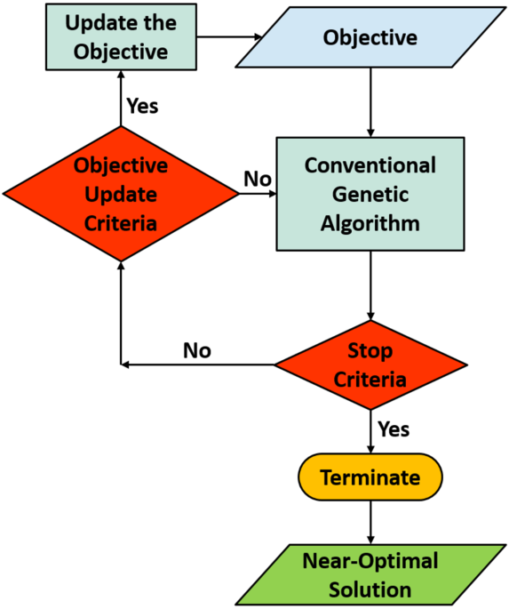
    Scientists have successfully employed an advanced design technique called the Adaptive Genetic Algorithm (AGA) to create novel materials known as metasurfaces, which can manipulate light in unprecedented ways. These metasurfaces, designed using the AGA method, tackle complex challenges in photonics with high-dimensional parameter spaces where traditional design methods fail.

    One notable achievement is the development of a reflectarray metasurface capable of steering light beams for telecommunications. This optimized design, overcoming limitations of conventional metasurfaces, exhibits high reflection efficiency and robustness against manufacturing imperfections. The AGA technique enabled the creation of a binary-pattern metasurface operating in the near-infrared regime, crucial for modern communication technologies.

    In another application, researchers engineered an innovative optical leaky-wave antenna that can independently direct two different polarizations of light. Traditional antennas have limitations in controlling the direction of multiple light modes simultaneously. The AGA method facilitated the design of an aperiodic grating antenna, allowing for tailored dual-beam radiation, a significant advancement for applications requiring precise light control.

    The AGA technique also led to the creation of compact birefringent metasurface unit-cells. These devices can manipulate different polarization components of light independently, with a reduced building block size compared to conventional dielectric metasurfaces. This breakthrough enables higher resolution and more compact optical devices with polarization-dependent functionalities.

    Furthermore, scientists designed a unique metasurface that is both transparent to visible light and highly absorptive in the infrared spectrum. This dual-band functionality is particularly relevant for solar cell technology. The metasurface can act as a cooling layer for solar cells by filtering out unwanted heat-generating infrared radiation while allowing visible light for energy conversion, potentially improving solar cell efficiency and longevity.

    Beyond specific applications, the research highlights the valuable data generated during the AGA optimization process itself. By analyzing the vast dataset of structural designs and their optical properties explored by the algorithm, researchers can gain deeper insights into the design space of metasurfaces. This “surplus data” can be leveraged for machine learning and artificial intelligence applications, potentially accelerating future discoveries in metamaterials and photonics. These findings demonstrate the power of the AGA technique in pushing the boundaries of metasurface design and opening new avenues for advanced optical technologies.

    Source link

  • Garmin Fenix 3 HR Unveiled: Optical Heart Rate & Software Update

    Garmin Fenix 3 HR Unveiled: Optical Heart Rate & Software Update

    Garmin has unveiled its latest fitness devices at CES, including the Fenix3 HR, the newest iteration of its popular Fenix3 multisport watch, now equipped with an optical heart rate sensor. The company also announced the Tactix Bravo, a new sibling to the Fenix3, and the Varia Vision heads-up display, detailed in a separate announcement.

    The Fenix3 HR integrates Garmin’s Elevate optical HR sensor, similar to the one in the FR235, allowing for continuous 24/7 heart rate monitoring during workouts and daily activities. This addition enables features like ‘Intensity Minutes’ tracking, aligning with health organization guidelines for weekly exercise. While the Fenix3 HR maintains the same width as the original Fenix3, it is slightly heavier by 6 grams. Battery life sees a reduction compared to the Fenix3, with GPS mode lasting 16 hours, UltraTrac GPS mode at 40 hours, and watch mode at 3 weeks. The Fenix3 HR is initially available in a grey color, with a bundle option including a HRM-RUN heart rate strap for advanced running dynamics and metrics such as HRV, Lactate Threshold, and Stress Score, which are not supported by the optical sensor alone. For swimming, a separate HRM-SWIM or HRM-TRI strap may be required as Garmin is still assessing the accuracy of the optical sensor in water. Initial testing of the Fenix3 HR’s optical sensor shows good performance in steady-state heart rate tracking, with a slight lag during interval training, consistent with the FR235. GPS accuracy during initial runs appears to be reliable.

    In addition to the Fenix3 HR, Garmin has introduced new band options for the Fenix3 line, including a lightweight Titanium band, and leather and nylon ‘fabric’ straps. The Titanium band aims to offer a lighter alternative to the existing metal band option. The new leather and nylon straps utilize a slip-through system for easy, tool-free band changes. These straps include brown leather, black nylon, and olive nylon options, alongside separately available lime green and blue silicone straps. These new additions expand the already extensive Fenix3 range, which includes numerous variations based on color, materials, and bundled accessories.

    Garmin will also release a software update for all existing Fenix3 watches, bringing new sports profiles and features. These include Stand Up Paddleboarding (SUP), Golf (with 40,000 course downloads), and Rowing modes, each with specific metrics. The update also adds Gen2 Running Dynamics, Lactate Threshold and Stress Score testing, Performance Condition metrics, Music Control, Audio Lap Alerts, Last Swim/Bike/Run and ‘My Day’ widgets, a Do Not Disturb mode, and Tactical & Jumpmaster apps, previously exclusive to the Tactix series. These software enhancements are expected to be available immediately, particularly for users already on the Fenix3 beta program.

    Finally, Garmin announced the Tactix Bravo, a successor to the original Tactix watch, aimed at military and law enforcement professionals. The Tactix Bravo builds upon the Fenix3 platform, incorporating features like a night vision goggle compatible display, non-reflective design, and specialized software modes including Jumpmaster and Tactical operations. In most other aspects, the Tactix Bravo shares feature parity with the Fenix3.

    Source link

  • Stanford Unveils Breakthrough Lightweight VR Headset Design

    Stanford University engineers have created a prototype for a significantly lighter virtual reality headset, weighing less than 2.5 ounces. This marks a considerable reduction in weight compared to many current VR devices. The headset achieves this lightweight design by employing pancake optics and a newly developed polarization-based optical element that serves as its display. This innovative display technology is designed to produce a nearly holographic visual experience, aiming for highly realistic 3D imagery. Researchers believe this breakthrough in weight reduction could lead to greater user comfort, enabling longer and more immersive VR sessions. The development is seen as a promising step toward making VR technology more practical and accessible for a wider range of applications, though it is currently a research prototype and not yet commercially available.

    Source link

  • New Study Reveals Latest OLED Optical Design Advances

    Recent advancements in the optical design of OLEDs are paving the way for brighter and more efficient displays, according to a new review article. OLED technology, known for its use in smartphones and televisions, faces ongoing challenges in maximizing light output. The review, published in Advanced Functional Materials, details significant progress made in the last decade in addressing this issue.

    Researchers, led by Salehi, highlight various optical design strategies that are boosting OLED performance. These techniques involve using microlenses, photonic crystals, plasmonic nanostructures, and metasurfaces. These methods work by carefully controlling light at a microscopic level, reducing internal reflections and extracting more light from the OLED material. This translates to displays that are not only brighter but also consume less power.

    The review suggests that these optical innovations are crucial for the future development of OLED technology and its wider application in displays and lighting. While progress is significant, the researchers emphasize that further research and development are needed to overcome remaining challenges and fully realize the potential of OLEDs for next-generation technologies.

    Source link

  • GW Engineers Design 3D-Printed Optical Mapping System

    Students at the George Washington University’s School of Engineering and Applied Science have designed a 3D-printed optical mapping system. This new device offers a low-cost and portable alternative to traditional, more expensive systems used for biological research. Optical mapping is a technique that allows researchers to study the electrical activity of cells and tissues, particularly in the heart. The student-designed system aims to make this technology more accessible to labs and research facilities. By utilizing 3D printing, they have created a system that is significantly more affordable and easier to use compared to commercially available options. This innovation is expected to enhance biological studies of cellular and tissue electrical function and could potentially lead to future clinical applications. The project was developed within the School of Engineering and Applied Science.

    Source link

  • Maxwell Breakthrough: Photonics Design Gets a Speed Boost

    Maxwell Breakthrough: Photonics Design Gets a Speed Boost

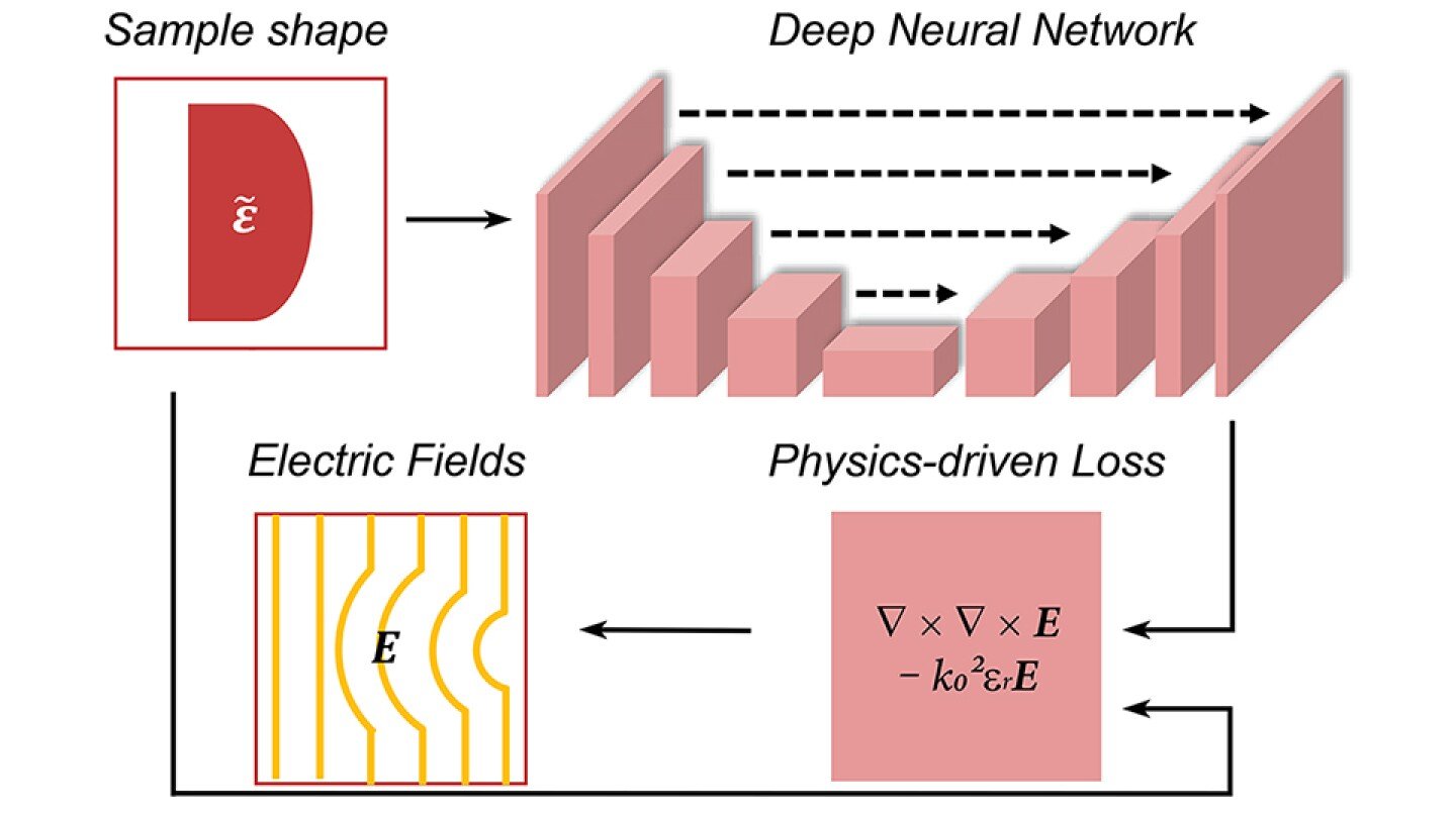
    Researchers have developed a deep neural network called MaxwellNet that can solve Maxwell’s equations with increased speed and accuracy. Maxwell’s equations are essential for designing optical elements within photonic devices. Traditional methods for optical design rely on simulations, often using the finite difference time domain (FDTD) method, which can be computationally demanding. To improve this process, researchers designed MaxwellNet, a deep neural network that uses a novel training approach. Unlike typical neural networks that learn from input-output datasets, MaxwellNet is trained by generating random outputs and then assessing if these outputs adhere to Maxwell’s equations. This assessment is done by calculating the residual error, which then guides the network’s learning process. This method of training by minimizing solution residuals, although new to solving Maxwell’s equations, has been applied in other fields like computational fluid dynamics. MaxwellNet requires an extended initial training period, but after this phase, it can rapidly and accurately simulate solutions for specific classes of optical components. In comparisons with a commercial finite element method solver, COMSOL, MaxwellNet demonstrated speed improvements of more than two orders of magnitude. The researchers also successfully designed an optical lens using MaxwellNet, and the results showed strong agreement with simulations from COMSOL. Future research aims to expand MaxwellNet to handle three-dimensional problems and incorporate nonlinear optical properties. The developers believe this innovative method will create new opportunities in photonics design and simulation.

    Source link