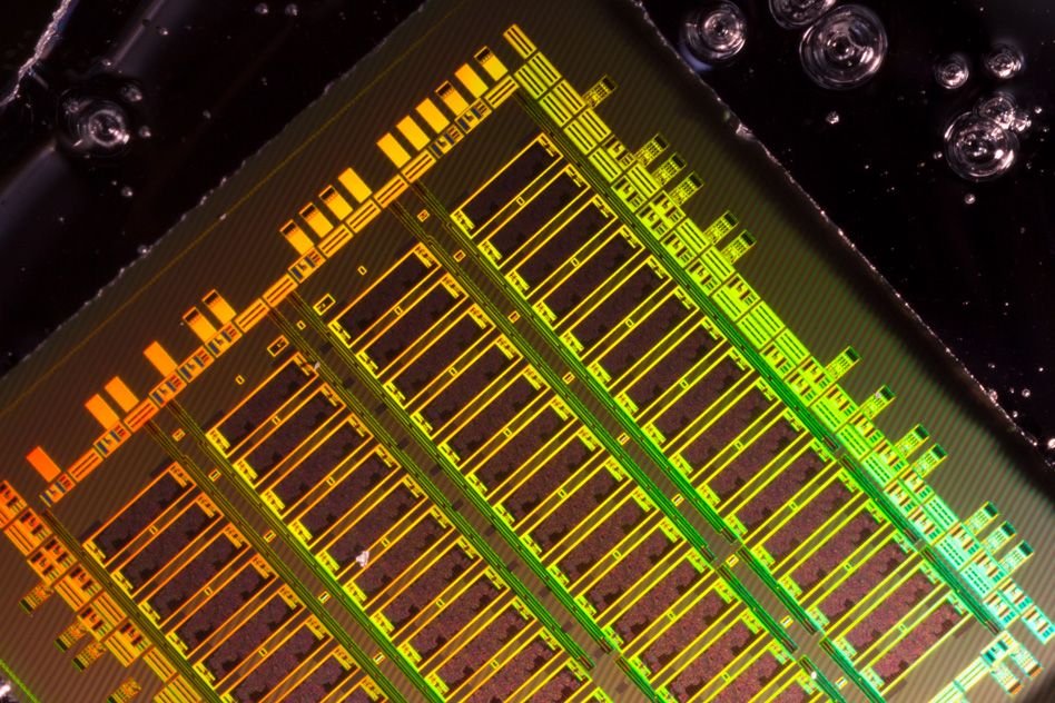
Researchers have achieved a new milestone in chip technology by developing a method to integrate optical and electronic components on a single chip using standard manufacturing processes, but now with the capability to build them separately and optimize each independently. This breakthrough, led by teams from MIT, the University of California at Berkeley, and Boston University, overcomes limitations of their previous approach which required using older chip technology. The new technique allows the use of more modern, high-performance transistor technologies while incorporating photonics. By separating the fabrication of electronics and photonics, chip manufacturers could add optical input and output to processors and GPUs without significant changes to existing production lines, potentially boosting performance through faster speeds and reduced power consumption. Optical communication on chips is seen as essential for future computing needs as energy demands rise with increasing transistor counts. This integrated approach dramatically reduces the power consumption and space of optical components compared to current market options. The researchers utilized polysilicon, deposited directly on glass, and experimented with different deposition methods at SUNY Polytechnic Institute to find a balance between electrical conductivity and optical efficiency in the material. This advancement promises to pave the way for more energy-efficient and faster computer chips by merging the advantages of optical communication with advanced microelectronics.

Leave a Reply