Researchers have developed a novel optimization algorithm to streamline the design of photonic devices, which are crucial components in technologies that manipulate light, such as advanced communication systems and sensors. Designing these devices traditionally involves a complex and time-consuming trial-and-error process. Engineers would manually propose a structure, simulate its interaction with light, and then tweak the design based on the simulation results. This process is not only inefficient but also relies heavily on intuition and limited automated methods.
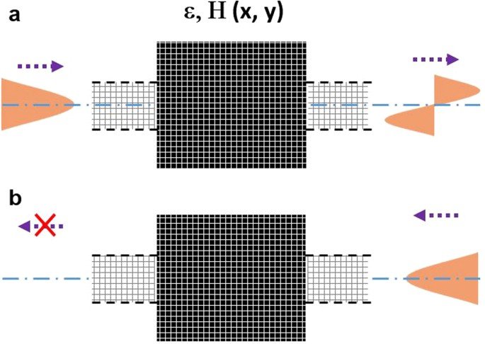
The new algorithm approaches the design problem by treating the device as a “black box” and directly optimizing for a desired light output. Instead of iteratively guessing structures, the algorithm works backward from the intended device function, such as specific spectral modulation or mode conversion. It mathematically defines the device’s objective, for example, achieving a particular magnetic field at its boundaries. Then, it iteratively refines both the device’s internal dielectric structure and the electromagnetic fields within it to match this objective, while simultaneously adhering to the fundamental laws of electromagnetism, known as Maxwell’s equations.
This iterative process is broken down into two steps. First, it assumes a dielectric structure and calculates the electromagnetic field that minimizes discrepancies within Maxwell’s equations. Second, it reverses the roles, optimizing the dielectric structure based on the previously calculated electromagnetic field. These steps are repeated, gradually converging toward a design that fulfills the objective. This “objective-first” approach is significantly faster and less computationally demanding than traditional methods, and it can handle more complex designs with greater freedom.
A key challenge in practical photonics is that devices are typically made from a limited number of materials, often just two, like silicon and air, creating a binary structure. The initial optimization algorithm generates structures with continuous variations in material properties, which are not directly fabricable. To address this, the researchers incorporated a “binarization” technique. This method encourages the algorithm to converge towards designs that are already close to a binary structure during the optimization process itself. By adding a cost function that favors binary solutions, the algorithm ensures that the device performance is maintained even when converted to a purely binary, manufacturable structure.
To test and evaluate their algorithm, the researchers performed computer simulations in two dimensions, focusing on the behavior of Transverse Electric fields. They simulated device performance under various conditions and assessed it using metrics like the physics residual (a measure of how well the design adheres to Maxwell’s equations), transmission efficiency in both directions (left-to-right and right-to-left), and a “binary coefficient” indicating how close the designed structure is to a perfect binary structure. This new algorithm represents a significant step forward in automated photonic device design, promising faster development and potentially enabling more complex and efficient optical technologies.
Leave a Reply